FIELD GUIDE / semiconductor materials
A Device Lying Flat Above a Kitchen
The silicon roof is not a passive slab of futuristic black glass. Its electrical behaviour moves with temperature, defects, contacts, and light, making the roof a device before it is a building material.
At a glance
- Silicon is a semiconductor whose carrier concentration and resistivity depend on temperature, doping, illumination, and material condition rather than a metal-like universal conductivity.
- Insulation reliability is governed by local electric field, geometry, voids, contamination, moisture, waveform, and conditioning rather than nominal voltage alone.
- A silicon material record requires crystal form, doping, carrier type, resistivity, measurement temperature, geometry, and realized layer or wafer form.
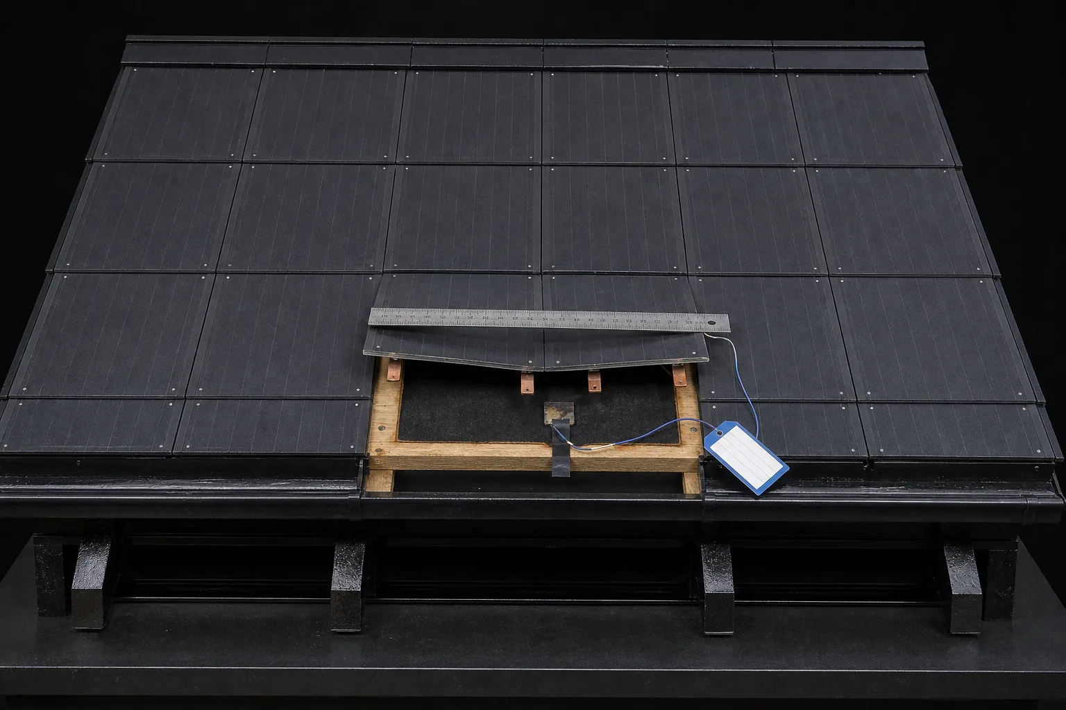
Upon a respectable suburban house there lies not shingles, nor slate, nor the modest corrugation which has protected roofs without offering opinions for generations, but a black roof of silicon.
Not panels mounted above the roof with their wiring tucked behind them, like a well-behaved appliance.
The roof itself: a broad exposed electrical surface, taking the day directly upon its back.
Its dark planes would receive the morning, the pollen, the rain, the pigeon, the ladder, and at noon the whole concentrated discourtesy of summer.
A silicon roof.
At first glance it would look admirably simple.
Silicon has the sober glamour of the computer age: dark, hard, precise, already entrusted with calculators, satellites, factories, and the small domestic tyranny of the doorbell camera.
One might suppose that a substance which runs electronics has settled, once and for all, the tiresome question of whether it conducts electricity.
But the roof would not be a sheet of black metal with ambitions.
It would be a semiconductor device, placed where all materials are least able to mind their own business: outdoors.
The trouble would begin not when the rain came, but when somebody called the thing a conductor.
But Is Silicon Not a Metal in a Black Coat?
No. This is the first correction, and it is owed the dignity of being made before the roof begins its more elaborate mischief.
Silicon does not conduct like copper with a degree in architecture.
It is an indirect semiconductor, and its intrinsic carrier concentration at room temperature is a statement about a specified condition of a specified crystal, before any practical device has supplied its doped regions, contacts, layers, fields and illumination.
The popular picture has taken a silicon chip, noticed that it does electrical things, and concluded that silicon is a metal in a dark overcoat.
The popular picture has, in this instance, arrived wearing the overcoat backwards.
A metal conductor is chosen for low bulk resistivity along a defined path.
Silicon is chosen because its carrier population can be engineered.
Those are different arguments, and the record for a semiconductor keeps them apart.
Carrier type, intentional dopant species, total chemical concentration, electrically active concentration, compensation, carrier concentration and resistivity are separate fields.
They are not ceremonial names for one number.
They are distinct chances for a roof to decline a simple story.
Even the shallow donor energies differ from one dopant species to the next, by amounts small in electronvolts and large in consequence.
A claim that silicon is simply “conductive” therefore resembles calling a violin simply “audible.”
It neglects the arrangement which causes the sound.
The Noon Sun Changes What Is Being Measured
It supplies light, certainly. It also supplies a thermal condition, and the latter has no obligation to behave like a helpful assistant.
The band gap of silicon is not a nameplate constant. Its accepted expression has temperature written into the definition, and it falls as the material warms.
A roof at one temperature and a roof at another are not the same roof in different weather.
They are electrically different roofs.
This is the noon inversion.
The dark surface looks most earnestly at work when the sun is strongest.
Yet visible brightness does not report junction temperature, carrier distribution, contact resistance, or the condition of a dielectric edge.
The roof may be receiving its great daily audience while its electrical quantities have quietly changed seats.
Metals have the same lesson in a simpler form. A metallic resistance element is modelled with a temperature coefficient, and even that approximation is only good across a modest span.
Silicon is not licensed to inherit a metal’s coefficient as though it were a photovoltaic one.
It merely shares the larger moral.
An electrical property without a stated temperature is a house key with no address.
The roof therefore needs a thermal model because it is an electrical object, not because heat has become picturesque.
Its actual condition depends on semiconductor composition and doping, on the illumination spectrum, on cell architecture, mounting, encapsulation, contacts, moisture and protection.
The honest conclusion is not a universal figure for noon output.
It is that an output claim without those particulars has arrived before its evidence.
A Silicon Roof Is Not One Material
Only in the way a city is one building.
Elemental silicon became the process platform partly because its crystal can be made in large characterized wafers and paired with its own oxide in a mature processing system.
But a semiconductor record must state more than a formula.
It needs the crystal phase, the material form, the composition, the doping profile, the defect context, and the difference between bulk, wafer, film and heterostructure.
Here is the rebuke a roof catalogue deserves.
A wafer 725 µm thick and an epitaxial layer 200 nm thick may share a formula and an orientation while being thoroughly different records.
For a wafer, the identity includes diameter, thickness, face orientation, dopant type, resistivity range, surface designation and lot traceability.
For a layer, it includes thickness, substrate, buffer stack, growth method, composition profile and strain state.
A brochure that says merely “silicon” has named the kingdom and omitted the address.
Even undoped is no refuge from this paperwork.
It means no intentional addition. It does not mean the demonstrable absence of all impurities.
A measured resistivity must travel with its temperature and its geometry, and any conversion from resistivity to carrier concentration must name the host, the dopant and the model used.
Silicon wafer reference materials exist, certified across several orders of magnitude of resistivity, with a full uncertainty analysis.
That does not make every commercial roof tile a reference artifact.
It makes precisely the opposite point. Measurement chains are important enough that somebody had to build one deliberately.
The silicon roof is therefore not a futuristic pane of glass.
It is a collection of specified regions and interfaces, attempting to remain a collection of specified regions and interfaces while exposed to weather.
Glass has never asked for a carrier profile.
Glass knows its place.
The Wire Can Be Fine While the Contact Misbehaves
Very easily. Indeed this is one of the domestic humiliations of electrical engineering.
A system may select excellent materials in bulk and then lose its dignity entirely at a small dirty meeting between them.
Copper’s bulk resistivity is one of the best-characterized numbers in engineering, and a long copper run has a perfectly predictable resistance.
But the power dissipated goes as the square of the current.
Ten times the current in the same conductor is a hundred times the heat, and a run that wasted a few tens of watts becomes a run wasting kilowatts.
The arithmetic is plain.
The roof connection is not.
Contact normal force, oxide disruption, surface contamination and fretting govern the constricted microscopic paths where two conductors actually meet.
A low-resistance copper route may therefore arrive at a termination and discover that its careful character has not been inherited by the handshake.
The connection hardware can add comparable heat, whenever contact resistance has been left out of the calculation.
This does not mean every roof connector is a fire waiting for a speech.
It means a connection must be a specified and inspected component, rather than an optimistic punctuation mark between two good conductors.
Heat at the contact is not refuted by the wire’s admirable bulk resistivity.
The wire has made one promise.
The contact has made another.
Insulation Cannot Be Judged by Thickness Alone
Thickness is an actor, but it is not the whole cast.
Twenty kilovolts across ten millimetres of ideal insulation gives an average of two kilovolts per millimetre.
Average is the word doing all the work.
A sharp conductor strand, a void, a conductive contamination, or a locally thin region can make the field there substantially higher.
The roof is no longer a flat black slab.
It has corners, penetrations, edges, wet surfaces, interfaces, and the small defects which insist on being local while everybody else is speaking in averages.
At an interface normal to the field, the layer of lower permittivity takes the higher field.
A void behaves like a low-permittivity inclusion.
It can therefore develop the more severe local field, and begin partial discharge, well before the surrounding insulation has come anywhere near its nominal strength.
The trapped bubble is stressed harder than the material around it. That is the whole difficulty in one sentence.
Air itself is insulating only under conditions. Its breakdown gradient moves with pressure, temperature, humidity, geometry, gap size and waveform.
The roof has accumulated, by now, an irritating number of variables.
It has also acquired the beginnings of honesty.
A Withstand Test Does Not Settle the Matter
It performs a valuable service, and it should not be asked to perform a supernatural one.
A high-voltage test can reveal whether a specimen survives, leaks, initiates partial discharge, or breaks down under defined conditions.
But the definition requires the thickness, the electrode shape, the voltage ramp rate, the waveform, the frequency, the temperature, the humidity, the immersion medium and the conditioning time.
A reported withstand voltage without those companions is not a conclusion.
It is an abandoned suitcase.
The photovoltaic testing guidance separates short-term intrinsic, thermal and electromechanical breakdown from the longer-term mechanisms: partial discharge, inclusions, electrical treeing and water treeing.
It identifies localized imperfections, and nonuniformity in the material or the test environment, as the common actual causes.
The roof does not necessarily fail with a grand flash across the whole surface.
It may instead conduct a small private argument at an edge, inside a void, or at a damaged interface.
That is another inversion. The roof is not chiefly betrayed by the broad heroic field imagined by the observer on the street.
It is betrayed by its exceptions: the defect, the contact, the contaminated path, the local field, the condition omitted from the shorthand.
Nor can a result measured on one thickness be multiplied through a thicker assembly to yield a larger safe voltage.
Breakdown is stochastic, and it varies as composition and structure vary.
This is not pessimism. It is a design method.
Specify the waveform, the duration, the geometry, the environmental conditioning, the failure probability and the failure mode.
Then the roof may be examined as an electrical device, rather than admired as a black architectural adjective.
And So the Roof Receives the Summer
Imagine it in the long afternoon.
The silicon lies dark beneath the sun. The house below it remains agreeably ordinary.
There is no blue corona playing across the gutters, no dramatic crackle, no heroic graph rising in the family room.
Nothing in particular occurs to the unaided eye, which is precisely why a visual impression is such a poor electrical instrument.
There will instead be records: the crystal and layer identity, the dopant and carrier data, the measurement temperatures, the contact condition, the insulation geometry, the test waveform, the humidity, the thermal condition and the protection arrangement.
There may be checks for changing insulation resistance, for temperature rise, for partial-discharge pulses or loss behaviour, each interpreted within a test method rather than mistaken for a direct reading of remaining life.
A silicon roof does not become a building material merely by lying flat above a kitchen.
It remains a device.
The day warms it. The light enters it. The contacts and the dielectric edges keep their small appointments with physics.
The useful question is not whether the roof looks like dark glass.
The useful question is what has been built beneath the dark surface, and under what conditions it agreed to behave.
AT THE BENCH
Questions, with the conditions attached.
Is silicon basically a metal because electronics run on it?
Silicon is a semiconductor, not a generic metal conductor. Its reported intrinsic carrier concentration is 1 x 10^10 cm^-3 at 300 K, and its electrical response changes with temperature, intentional dopants, compensation, defects, illumination, and device structure. A silicon roof therefore requires a specified cell and interconnect design; elemental silicon alone does not establish electrical output or fault behaviour.
Why does a hot silicon roof need an electrical model as well as a roofing model?
A silicon photovoltaic roof contains temperature-sensitive semiconductor regions, current paths, contacts, and dielectric layers. Silicon’s band-gap record is temperature-dependent, and resistivity measurements also require stated temperature and geometry. Heating can therefore change the conditions under which carriers, junctions, contacts, and insulation operate. A roof surface that looks bright and intact does not by itself establish its electrical condition.
What information has to identify a silicon roof material properly?
A usable semiconductor record states formula, crystal phase, material form, dopant type, carrier type, resistivity range, measurement temperature, and the realized geometry. A 725 µm silicon wafer and a 200 nm epitaxial layer can share formula and orientation while remaining different records. A photovoltaic roof also needs its cell architecture, layer stack, contacts, encapsulation, and electrical protection specified separately.
Does a dopant concentration tell the whole electrical story?
No. Intentional dopant species, total chemical concentration, electrically active concentration, compensation, mobile carrier concentration, and resistivity are separate fields. NIST reference curves for boron- and phosphorus-doped silicon cover 10^13 to 10^20 cm^-3 and use data fitted at 23 °C and 27 °C. A quoted concentration without host, dopant, method, temperature, and measurement basis does not determine roof electrical behaviour.
Can low-resistance wiring still become a hot fault?
Yes. Bulk resistance governs only part of a current path. Contact normal force, oxide disruption, surface contamination, and fretting control the microscopic paths through a connection and can add heat that a wire calculation omits. The electrical loss follows P = I^2R, so a local contact resistance can become consequential as current rises even when the adjoining conductor has low bulk resistivity.
Why is a tiny void in roof insulation a serious electrical detail?
A void behaves approximately as a low-permittivity inclusion, so it can take a higher local electric field than surrounding insulation. OpenStax examples list air at relative permittivity 1.00059 and representative strength 3 x 10^6 V m^-1, compared with Teflon at 2.1 and 60 x 10^6 V m^-1. Local field intensification can initiate partial discharge before the surrounding solid reaches its nominal strength.
Does a dielectric withstand number tell how much voltage a roof can always take?
No. A dielectric-breakdown result depends on thickness, electrode shape, waveform, frequency, voltage ramp, temperature, humidity, immersion medium, conditioning time, stressed volume, and acceptable failure probability. A reported 20 kV mm^-1 result cannot simply be scaled into a claim that a 2 mm assembly is safe at 40 kV. Breakdown is a test outcome, not a universal voltage passport.
What does temperature change in an electrical material?
Temperature can change resistance, carrier behaviour, band structure, contact response, and dielectric reliability. The local resistance relation R(T) ≈ R0[1 + α(T − T0)] is only a limited-range model, and semiconductor parameters need their measurement temperature stated. Silicon’s reported band-gap relation uses temperature in kelvin, so a room-temperature silicon value cannot be silently used as a high-temperature device guarantee.
Why cannot a claim about elemental silicon prove a photovoltaic roof claim?
Elemental silicon identifies neither a complete photovoltaic device nor its operating performance. Silicon is an indirect-gap semiconductor at 300 K and can be paired with silicon dioxide in a mature process system, but a roof also contains realized doped regions, interfaces, metal contacts, dielectric layers, encapsulation, and protection. Device architecture and conditions determine the component-level result.
What should be checked after a silicon roof has been hot for a long time?
An electrical reliability check records the relevant temperature, insulation resistance or loss behaviour, contact condition, local heating, and any partial-discharge or leakage evidence appropriate to the assembly. Those indicators require a defined test method and failure model; they are not direct readings of remaining dielectric strength. The useful result connects the observed condition to the particular layer stack, geometry, environment, and protection design.
Is higher sunlight automatically evidence that a roof is electrically safer or more productive?
No. Illumination is one operating condition among temperature, spectrum, semiconductor composition, doping, device architecture, contact design, and insulation condition. More visible brightness does not identify the temperature of the electrical stack, the carrier response of the junction, the resistance of a connection, or the local field at a dielectric defect. A production claim needs primary device data under stated conditions.